This details the hardware design for a simple 12-bit microporcessor. I created it for an undergraduate class which I took a few years ago. It is not really usefull for anything besides learning how computer hardware works, but I still think that it is pretty cool. I found the documentation for it on my hard drive and remebered how proud I was to have actually completed it; I am a computer scientist, not a computer engineer. Simple logic gates are used as the basis for the creation of more complex digital electronic circuits; those circuits, including a control unit, are in turn connected via a datapath to form a completed processor. The processor datapath is designed to implement the Simple-12 instruction set.
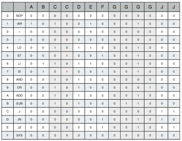
The Simple-12 processor is a 12-bit single-cycle, meaning that each instruction takes a full cycle to complete, processor with a very basic set of capabilities. The processor is designed to accept 12-bit instructions which are each composed of a 4-bit operation code and an 8-bit address. The instructions are fetched from a bank of instruction memory which is separated from another bank of data memory. Three registers are used in the processor for the program counter, accumulator, and indirect addressing resolver. The processor utilizes multiplexors switched from a central control unit to establish the correct datapath for a given instruction. A simple incrementer is used for the normal advancement of the program counter, while a full arithmetic logic unit is at the center of the processor.
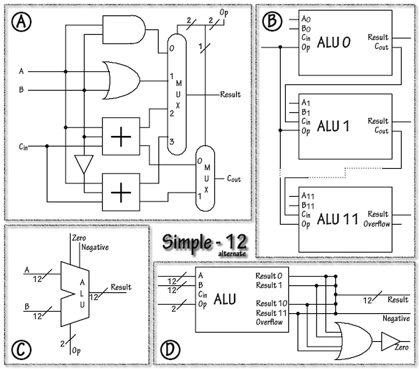
To build the arithmetic logic unit a 1-bit adder and 1-bit multiplexer are first created as shown below.
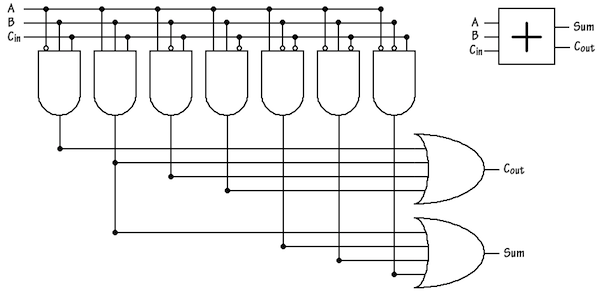
The above circuits are joined with additional logic gates to create a 1-bit ALU (figure A) which can perform addition, subtraction, and-ing, and or-ing. A 2-bit operation code is used to determine the mode and a flag is available to invert the B input to facilitate subtraction. Twelve of those 1-bit ALUs are joined to form a 12-bit ripple-carry ALU (figure B). Then, a nor operation is performed on all 12 output bits to create a zero flag, and the negative bit is tapped to create a negative flag (figure D) resulting in the final ALU (figure C).
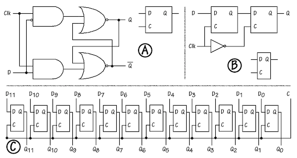
Memory is required for the registers. Logic gates are first used to create a 1-bit D-latch (figure A), and the D-latch is then used to create a 1-bit D-flip-flop (figure B). This memory is emits data at the beginning of the clock cycle and stores data at the end, which makes it perfect for registers in a single cycle processor. The D-flip-flops are arranged in parallel to form a 12-bit wide word (figure C). Each of the three registers will use one of these.
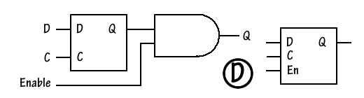
To create instruction and data memory logic gates are again used to create a 1-bit D-latch. An AND gate is added to create an enable flag (figure D). The enable flag must be set in order for data to be output.
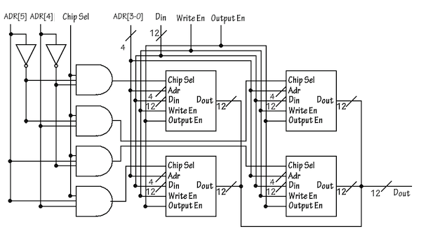
The 1-bit memory circuits shown above are next arranged into a 12-bit wide and 4-word deep matrix where. A 2-bit address is sent to the 4 by 12 module and processed by selection logic to determine which word to select.
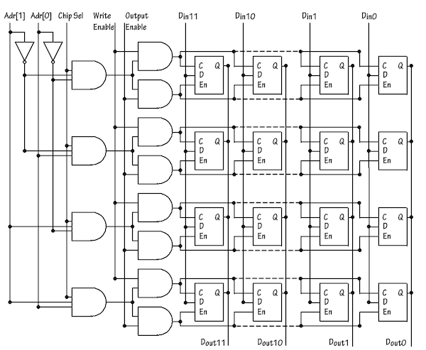
The 4-word memory module above can then be used in a matrix to produce a 16 word memory module.
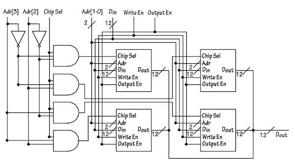
That same process can be used again on the resulting 16 word memory module to create a 64 word memory bank, two of which will be required (bits 6 and above are ignored).
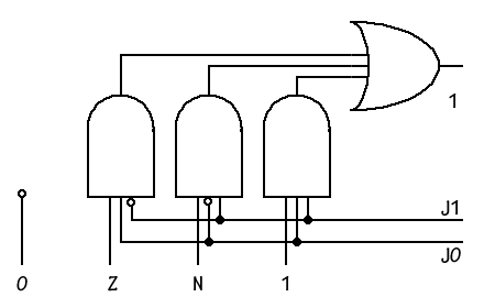
Logic is required allow the jump address to be sent to the program counter when the ALU evaluates a branch or jump instruction.
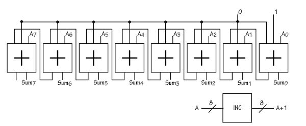
A simple incrementer is also needed for normal advancement of the program counter.
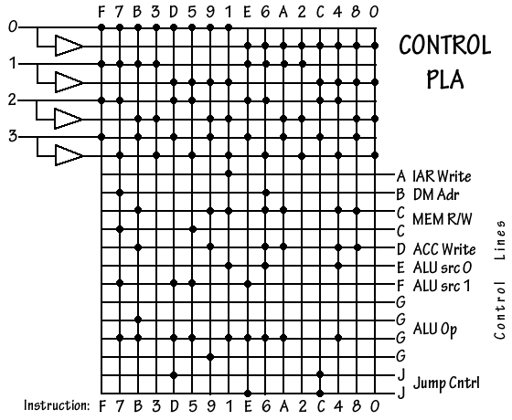
The final component is a programable logic array (PLA) to be used as the control unit.
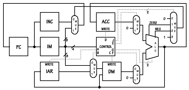
With all the components designed the datapath can be assembled (see end). The diagram should be easily understandable, possibly except for the IAR register and the jump circuit. The IAR register receives the memory address to be accessed during indirect memory addressing. When the jump circuit is activated by way of the appropriate control lines it instructs the multiplexor feeding the program count register to use the supplied jump address when the ALU sig- nals wither negative or zero.
On each cycle the program counter is read (100ps), the instruction memory is ready (200ps), then data memory is read (200ps), the ALU is used (200ps), and then either memory or registers are written (200ps or 100ps). Assuming that the multipexors and control unit have no measurable delay, the maximum access time is 900ps per cycle or 1.1GHz.
The design of this processor does not include a mechanism for handling arithmetic over- flows, this should be the first improvement made to the design. The design could also be improved by implementing pipelining; to do so additional control logic would be needed to forward data in the pipeline and to stall the pipeline when potential conflicts would occur.
The Simple-12 processor outlined in this document is indeed a very simplistic processor, but it demonstrates many of the key features of actual production microprocessors and give the pro- grammer an understanding of what is happing at the lowest level of hardware.